RAM Fundamentals
"RAM" isn't one technology — it's a family. The RAM that makes up multi-gigabyte main memory (DRAM) and the RAM that makes up tiny, ultra-fast on-chip caches and registers (SRAM) trade off density and cost against speed and simplicity in almost opposite ways. Understanding why they differ explains a lot about the memory hierarchy: it's not that engineers chose to make caches small, it's that the technology fast enough to keep up with a CPU core physically cannot be made cheap and dense enough to serve as multi-gigabyte main memory.
Core Concepts
| Term | Meaning |
|---|---|
| SRAM (Static RAM) | Memory built from bistable transistor circuits (typically six transistors per bit) that hold their value as long as power is applied — no refresh needed. |
| DRAM (Dynamic RAM) | Memory that stores each bit as charge on a tiny capacitor, accessed through one transistor per cell — far denser than SRAM, but the charge leaks away and must be periodically refreshed. |
| Refresh | The periodic read-then-rewrite cycle DRAM needs to restore leaking capacitor charge before the stored value is lost (JEDEC DRAM parts are typically specified around a 64 ms refresh window per row). |
| Memory controller | The hardware (on-die on modern CPUs) that issues commands to DRAM chips — activate a row, read/write a column, refresh — and manages timing. |
| Memory channel | An independent electrical path between the memory controller and DRAM modules; more channels roughly multiply available bandwidth. |
| DIMM | Dual In-line Memory Module — the physical stick of DRAM chips plugged into a motherboard. |
Mechanism
Why SRAM vs. DRAM at different tiers
| SRAM — registers, L1/L2/L3 | DRAM — main memory | |
|---|---|---|
| Cell | ~6 transistors/bit | 1 transistor + 1 capacitor per bit |
| Refresh | Not needed | Required periodically |
| Density & cost | Low density, expensive per bit | High density, cheap per bit |
| Speed | Fast | Slower |
A DRAM cell stores a bit as the presence or absence of charge on a capacitor; a single access transistor connects that capacitor to a bit line when its row is activated. Reading a DRAM cell is destructive — it drains the capacitor's charge — so the memory controller must sense the value with a sense amplifier and immediately write it back. This same read-sense-rewrite machinery is reused to implement periodic refresh: the controller works through the chip's rows in the background, refreshing each one before its charge decays enough to flip the stored bit. SRAM's six-transistor bistable cell holds its state electrically as long as power is supplied, so it needs none of this — at the cost of roughly 4-6x the transistors (and therefore silicon area and dollars) per bit compared to DRAM's one transistor and one capacitor. That density/cost difference is exactly why SRAM is used only where a small amount of memory must be extremely fast (registers, L1/L2/L3 caches) and DRAM is used for everything that needs to be large (main memory).
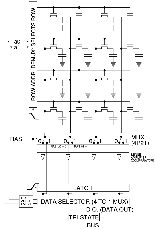
This layout explains the timings on the next section's spec sheets. A read activates a whole row at once, so the first access to a row pays the full row-activation cost while subsequent accesses to the same row (a "row hit") only pay the column select — which is precisely why sequential access patterns are so much faster than random ones, at the DRAM level as much as at the cache level.
DDR generations
Standard main-memory DRAM is specified by JEDEC as DDR SDRAM (Double Data Rate Synchronous DRAM) — "double data rate" because it transfers data on both the rising and falling edge of the clock. Each generation roughly doubles peak per-pin transfer rate and lowers operating voltage compared to the last, while adding capacity and reliability features:
| Generation | JEDEC standard | Typical data rate range | Notable changes |
|---|---|---|---|
| DDR3 | JESD79-3 | ~800-2133 MT/s | 1.5 V (1.35 V low-voltage variants) |
| DDR4 | JESD79-4 | ~1600-3200 MT/s | 1.2 V; bank groups for more parallelism |
| DDR5 | JESD79-5 | ~4800-8800+ MT/s | 1.1 V; on-die ECC; two independent 32-bit sub-channels per DIMM |
Newer generations aren't purely a speed upgrade for a given part — a higher data rate alone doesn't help if the CPU's memory controller can't issue enough concurrent requests, which is why per-generation architectural changes (like DDR5 splitting each DIMM into two independent sub-channels) matter as much as the raw MT/s number.
Channels and bandwidth
A single memory channel connects the controller to one or more DIMMs and has a fixed data width (64 bits per classic DDR4 channel, split into two 32-bit sub-channels for DDR5). Peak bandwidth is approximately:
bandwidth ≈ (data rate in transfers/sec) × (channel width in bytes)
Running two, four, or more channels in parallel (dual-channel, quad-channel, and the many-channel configurations used in servers) multiplies available bandwidth roughly linearly — one reason server/workstation CPUs expose far more memory channels than consumer chips.
Practical Usage
Most application code never talks to DRAM directly, but memory layout still determines how well it uses the channels and rows available:
// Sequential access: each cache-line-sized chunk is likely already
// in an open DRAM row/bank, and prefetchers can predict the pattern.
for (int i = 0; i < n; ++i) {
    sum += data[i];
}

// Strided/random access: each access may require the memory
// controller to close one row and open another ("row buffer miss"),
// which is measurably slower than staying within an open row.
for (int i = 0; i < n; ++i) {
    sum += data[shuffled_index[i]];
}
This is the DRAM-level version of the same locality principle that motivates CPU caches (see CPU Caches): sequential, predictable access patterns let both the cache hierarchy and the DRAM row buffer do their job well.
Edge Cases & Pitfalls
Refresh briefly makes a row unavailable for normal access, and refresh traffic scales with DRAM density. On mainstream systems this overhead is a small, well-amortized background cost — but it's part of why simply adding more DRAM capacity doesn't scale bandwidth for free, and it matters more on very large, high-density server memory configurations.
- DDR generations are not backward compatible electrically or physically (different voltages, pin-outs, and notch positions) — you cannot mix DDR4 and DDR5 modules or put a DDR5 DIMM in a DDR4 slot.
- More channels help only if the workload actually generates enough concurrent, independent memory requests; a single memory-bound thread with a serial dependency chain may not saturate even one channel.
- "Faster RAM" (higher MT/s) and "lower-latency RAM" (lower CAS latency in nanoseconds) are different axes — a higher data-rate module isn't automatically lower-latency in absolute time.
Comparisons
| Property | SRAM | DRAM |
|---|---|---|
| Cell structure | ~6 transistors, bistable | 1 transistor + 1 capacitor |
| Needs refresh? | No | Yes |
| Density | Low | High |
| Cost per bit | High | Low |
| Typical use | Registers, L1/L2/L3 cache | Main memory (DIMMs) |
| Access latency | Sub-nanosecond to a few ns | Tens of nanoseconds |
References
- JEDEC, DDR4 SDRAM Standard (JESD79-4) and DDR5 SDRAM Standard (JESD79-5) — official specifications.
- Memory refresh — Wikipedia — DRAM refresh mechanics.
- Patterson & Hennessy, Computer Organization and Design — memory technology chapter (SRAM/DRAM tradeoffs, DDR).
Books & Videos
- Ulrich Drepper, "What Every Programmer Should Know About Memory" — deep, still-relevant technical treatment of DRAM internals and memory controllers.
- Bryant & O'Hallaron, Computer Systems: A Programmer's Perspective — "The Memory Hierarchy" chapter covers RAM technology alongside caches.
- Computerphile, "How CPU Memory & Caches Work" — Matt Godbolt walks through the RAM-to-cache relationship.